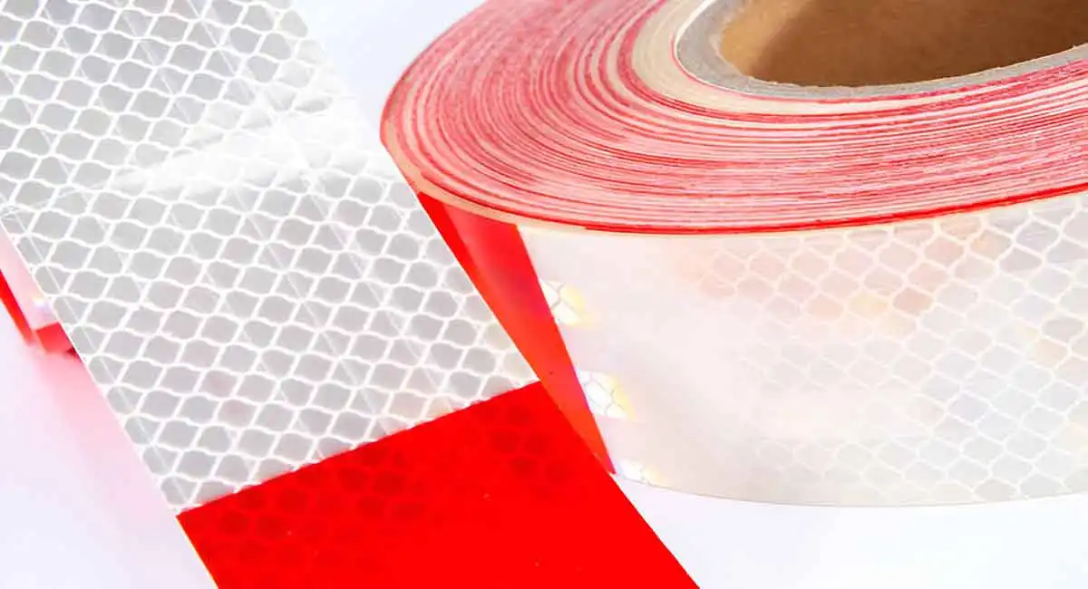
High-precision prismatic reflective sheeting : How to achieve efficient mass production, high precision and high consistency?

A prism is an object surrounded by two intersecting but non-parallel planes, used to split or disperse light beams, and is usually made of transparent materials (such as glass, crystal, etc.). In modern life, prisms are widely used in traffic road safety.
The above applications have high requirements for the surface shape and finish of micro prisms, usually requiring the surface shape to be λ/4-λ/10. In the production of ordinary prisms, manufacturers mostly use traditional grinding and polishing methods to process optical surfaces, but this process faces huge challenges in the production of prismatic reflective sheeting . Although some manufacturers can use advanced cutting methods to manufacture micro prisms of various lengths, there is no better processing method for optical surfaces to achieve large-scale, high-precision production, and there is no economical method to meet the huge market demand.
What is the traditional technology like?

The traditional grinding and polishing method for processing optical surfaces basically requires the use of support and optical glue technology. This method has a long production process and consumes a lot of support during product processing, resulting in high overall production costs and low efficiency. This process also requires a high level of technical skills of operators, and the cost of personnel training required by the company also increases accordingly; if the turnover of personnel is fast, it may cause problems such as poor product consistency and unstable quality.
Hangzhou Xingwei uses its own wafer-level synchronous structured process platform to process micro-prism products, combining advanced laser hidden cutting technology and CNC technology, high-precision and high-reliability micro-nano measurement technology to achieve the premise of ensuring technical indicators, greatly improve production efficiency and reduce production costs.
Wafer-level synchronous structured micro-nano optical preparation technology
Micro-nano optical devices are prepared using wafer-level synchronous structured technology. The materials can be glass, fused quartz, silicon, calcium fluoride and other inorganic materials. Micro-optical wafers with a maximum size of 300mm x 300mm can be produced. Only two steps are required to produce tens of thousands of high-quality micro-optical lenses. This production technology is highly scalable and cost-effective, suitable for ultra-large-scale production. The unique performance and cost advantages of this production technology have been fully demonstrated in fiber laser pumping applications: it has become the world’s main supplier of fast axis collimators (FAC),
Use wafer-level synchronous structuring technology to mass-produce high-precision micro prismatic
Prism micro-optical wafers
In the past, wafer-level synchronous structuring technology was more used in the production and preparation of cylindrical mirrors. When this technology is innovatively applied to the production and preparation of prismatic reflective sheeting . it can not only process micro-prism units with the same or variable periods on large-size optical wafers (such as 300mm X 300mm), but also has excellent consistency and extremely high processing efficiency, and can ensure angular accuracy and surface accuracy. This processing method is more than 10 times more efficient than traditional grinding and polishing processes, and the product consistency is high. The precision meets the requirements of many industries and effectively solves the pain points of the industry.
For example, in the field of optical communications, the company prepares 3 or more micro prismatic sheeting and special-shaped mirrors (examples are as follows) on the same micro-optical wafer at the same time according to customer needs, and the tolerance of each angle is controlled at ±0.01°, and the optical effective area PV<0.16um. We believe that high-precision prismatic reflective sheeting mass-produced using wafer-level synchronous structuring technology will have the potential to expand into more and newer application areas.


